 High frequency millimeter-wave PCB is composed of high-frequency circuit and the control circuit into a single unit. In addition, although high-frequency materials (PTFE, LCP, PPE, Low-k Epoxy) are more expensive than ordinary substrate materials, GLOBAL SUCCESS developed hybrid stack-up PCBs by creating the lamination and non-hole structure of high-frequency materials and ordinary materials (FR-4) with our proprietary technology.
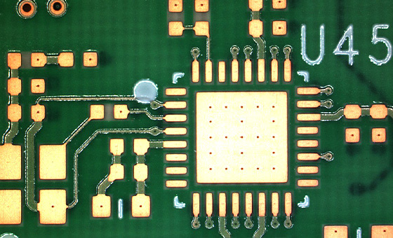
This high frequency millimeter-wave PCB lowers cost, supports a multi-layer stackup, and improves wiring freedom for high-frequency PCBs.
Features
Lower cost
Thinning and downsizing support
Reduction in transmission loss of high-frequency signals
Stabilization of high-frequency characteristics
Applications

Stackup

Electrical characteristics


